- 您现在的位置:买卖IC网 > Sheet目录336 > LCMXO2280C-C-EVN (Lattice Semiconductor Corporation)BOARD CONTROL EVAL MACHXO
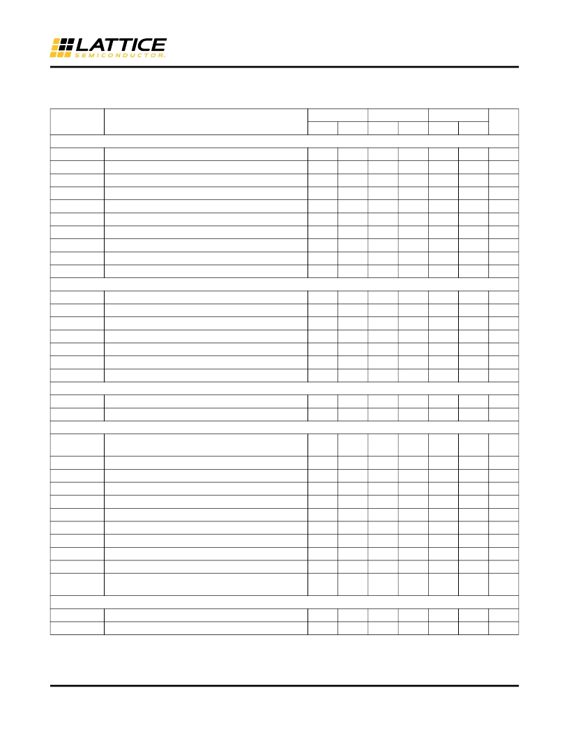
DC and Switching Characteristics
MachXO Family Data Sheet
MachXO Internal Timing Parameters 1
Over Recommended Operating Conditions
-5
-4
-3
Parameter
Description
Min.
Max.
Min.
Max.
Min.
Max.
Units
PFU/PFF Logic Mode Timing
t LUT4_PFU
t LUT6_PFU
t LSR_PFU
t SUM_PFU
t HM_PFU
t SUD_PFU
t HD_PFU
t CK2Q_PFU
t LE2Q_PFU
t LD2Q_PFU
LUT4 delay (A to D inputs to F output)
LUT6 delay (A to D inputs to OFX output)
Set/Reset to output of PFU
Clock to Mux (M0,M1) input setup time
Clock to Mux (M0,M1) input hold time
Clock to D input setup time
Clock to D input hold time
Clock to Q delay, D-type register configuration
Clock to Q delay latch configuration
D to Q throughput delay when latch is enabled
—
—
—
0.10
-0.05
0.13
-0.03
—
—
—
0.28
0.44
0.90
—
—
—
—
0.40
0.53
0.55
—
—
—
0.13
-0.06
0.16
-0.03
—
—
—
0.34
0.53
1.08
—
—
—
—
0.48
0.64
0.66
—
—
—
0.15
-0.07
0.18
-0.04
—
—
—
0.39
0.62
1.26
—
—
—
—
0.56
0.74
0.77
ns
ns
ns
ns
ns
ns
ns
ns
ns
ns
PFU Dual Port Memory Mode Timing
t CORAM_PFU
t SUDATA_PFU
t HDATA_PFU
Clock to Output
Data Setup Time
Data Hold Time
—
-0.18
0.28
0.40
—
—
—
-0.22
0.34
0.48
—
—
—
-0.25
0.39
0.56
—
—
ns
ns
ns
t SUADDR_PFU Address Setup Time
-0.46
—
-0.56
—
-0.65
—
ns
t HADDR_PFU
Address Hold Time
0.71
—
0.85
—
0.99
—
ns
t SUWREN_PFU Write/Read Enable Setup Time
-0.22
—
-0.26
—
-0.30
—
ns
t HWREN_PFU
Write/Read Enable Hold Time
0.33
—
0.40
—
0.47
—
ns
PIO Input/Output Buffer Timing
t IN_PIO
t OUT_PIO
Input Buffer Delay
Output Buffer Delay
—
—
0.75
1.29
—
—
0.90
1.54
—
—
1.06
1.80
ns
ns
EBR Timing (1200 and 2280 Devices Only)
t CO_EBR
t COO_EBR
t SUDATA_EBR
t HDATA_EBR
Clock to output from Address or Data with no output
register
Clock to output from EBR output Register
Setup Data to EBR Memory
Hold Data to EBR Memory
—
—
-0.26
0.41
2.24
0.54
—
—
—
—
-0.31
0.49
2.69
0.64
—
—
—
—
-0.37
0.57
3.14
0.75
—
—
ns
ns
ns
ns
t SUADDR_EBR Setup Address to EBR Memory
-0.26
—
-0.31
—
-0.37
—
ns
t HADDR_EBR
Hold Address to EBR Memory
0.41
—
0.49
—
0.57
—
ns
t SUWREN_EBR Setup Write/Read Enable to EBR Memory
-0.17
—
-0.20
—
-0.23
—
ns
t HWREN_EBR
t SUCE_EBR
t HCE_EBR
t RSTO_EBR
Hold Write/Read Enable to EBR Memory
Clock Enable Setup Time to EBR Output Register
Clock Enable Hold Time to EBR Output Register
Reset To Output Delay Time from EBR Output Regis-
ter
0.26
0.19
-0.13
—
—
—
—
1.03
0.31
0.23
-0.16
—
—
—
—
1.23
0.36
0.27
-0.18
—
—
—
—
1.44
ns
ns
ns
ns
PLL Parameters (1200 and 2280 Devices Only)
t RSTREC
t RSTSU
Reset Recovery to Rising Clock
Reset Signal Setup Time
1.00
1.00
—
—
1.00
1.00
—
—
1.00
1.00
—
—
ns
ns
1. Internal parameters are characterized but not tested on every device.
Rev. A 0.19
3-12
发布紧急采购,3分钟左右您将得到回复。
相关PDF资料
LDB100-024SW
LED POWER SUPPLY 24V 0-4A 100W
LDB150-048SW
LED POWER SUPPLY 24V-48V 3.125A
LDB200-048SW
LED POWER SUPPLY 24V-48V 4.2A
LDB75-048SW
LED POWER SUPPLY 24V-48V 1.56A
LDS8141-002-T2
IC LED DRIVER WHIT BCKLGT 16WQFN
LDS8160-002-T2
IC LED DVR WHT/RGB BCKLGT 16WQFN
LDS8620-002-T2
IC LED DRIVER FLASH 16WQFN
LDS8621002-T2-960
IC LED DRIVER FLASH 16WQFN
相关代理商/技术参数
LCMXO2280C-L-EV
功能描述:可编程逻辑 IC 开发工具 MachXO 2280C Eval Br d - Standard RoHS:否 制造商:Altera Corporation 产品:Development Kits 类型:FPGA 工具用于评估:5CEFA7F3 接口类型: 工作电源电压:
LCMXO2280C-M-EVN
功能描述:可编程逻辑 IC 开发工具 MachXO Mini Dev Kit RoHS:否 制造商:Altera Corporation 产品:Development Kits 类型:FPGA 工具用于评估:5CEFA7F3 接口类型: 工作电源电压:
LCMXO2280E-3B256C
功能描述:CPLD - 复杂可编程逻辑器件 2280 LUTs 211 I/O 1.2V -3 SPD
RoHS:否 制造商:Lattice 系列: 存储类型:EEPROM 大电池数量:128 最大工作频率:333 MHz 延迟时间:2.7 ns 可编程输入/输出端数量:64 工作电源电压:3.3 V 最大工作温度:+ 90 C 最小工作温度:0 C 封装 / 箱体:TQFP-100
LCMXO2280E-3B256I
功能描述:CPLD - 复杂可编程逻辑器件 2280 LUTs 211 I/O 1.2V -3 SPD
RoHS:否 制造商:Lattice 系列: 存储类型:EEPROM 大电池数量:128 最大工作频率:333 MHz 延迟时间:2.7 ns 可编程输入/输出端数量:64 工作电源电压:3.3 V 最大工作温度:+ 90 C 最小工作温度:0 C 封装 / 箱体:TQFP-100
LCMXO2280E-3BN256C
功能描述:CPLD - 复杂可编程逻辑器件 2280 LUTs 211 I/O 1.2V -3 SPD
RoHS:否 制造商:Lattice 系列: 存储类型:EEPROM 大电池数量:128 最大工作频率:333 MHz 延迟时间:2.7 ns 可编程输入/输出端数量:64 工作电源电压:3.3 V 最大工作温度:+ 90 C 最小工作温度:0 C 封装 / 箱体:TQFP-100
LCMXO2280E-3BN256I
功能描述:CPLD - 复杂可编程逻辑器件 2280 LUTs 211 I/O 1.2V -3 SPD
RoHS:否 制造商:Lattice 系列: 存储类型:EEPROM 大电池数量:128 最大工作频率:333 MHz 延迟时间:2.7 ns 可编程输入/输出端数量:64 工作电源电压:3.3 V 最大工作温度:+ 90 C 最小工作温度:0 C 封装 / 箱体:TQFP-100
LCMXO2280E-3FT256C
功能描述:CPLD - 复杂可编程逻辑器件 2280 LUTs 211 IO 1.2 V -3 Spd
RoHS:否 制造商:Lattice 系列: 存储类型:EEPROM 大电池数量:128 最大工作频率:333 MHz 延迟时间:2.7 ns 可编程输入/输出端数量:64 工作电源电压:3.3 V 最大工作温度:+ 90 C 最小工作温度:0 C 封装 / 箱体:TQFP-100
LCMXO2280E-3FT256I
功能描述:CPLD - 复杂可编程逻辑器件 2280 LUTs 211 IO 1.2 V -3 Spd I
RoHS:否 制造商:Lattice 系列: 存储类型:EEPROM 大电池数量:128 最大工作频率:333 MHz 延迟时间:2.7 ns 可编程输入/输出端数量:64 工作电源电压:3.3 V 最大工作温度:+ 90 C 最小工作温度:0 C 封装 / 箱体:TQFP-100
